Home>>User Support>>DDC Theory
Digital Down Conversion (DDC) Theory
Introduction
The HERON-FPGA family is ideal for many of the building blocks of digital communications. Providing large easily-programmed gate arrays, often combined with interface elements like ADC or DACs, they can be used to implement many system components.
The availability of hardware such as the HERON system is enabling designers to build radio systems where more and more of the system is digital. This often requires new techniques and terminology. This is an introduction to one such technique – the Digital Down Converter, or DDC.
This paper is not meant as a definitive reference on DDCs. Instead, it is a grounding in the basic concepts. It is enough for an experienced signal processing engineer to build his own DDC, but we have also provided references to other information sources for further reading.
The Digital Down Converter or DDC
A fundamental part of many communications systems is Digital Down Conversion (DDC). Digital radio receivers often have fast ADC converters delivering vast amounts of data; but in many cases, the signal of interest represents a small proportion of that bandwidth. A DDC allows the rest of that data to be discarded, allowing more intensive processing to be performed on the signal of interest.
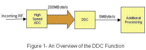
As an example, consider a radio signal lying in the range 39-40MHz. The signal bandwidth is 1MHz. However, it is often digitised with a sampling rate over 100MHZ, representing in the region of 200Mbyte/second.
The DDC allows us to select the 39-40MHz band, and to shift its frequency down to baseband. Once this is complete, the sampling rate can be reduced – with a 1MHz bandwidth, a sampling rate of 2.5MHz would be fine - giving a data rate of only 5Mbyte/second. This is shown in Figure 1.
How It Works
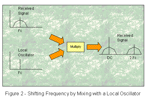
A DDC works by first shifting the bandwidth of interest to baseband by multiplying the received signal by a close approximation to the original carrier. This works on the (simplified) mathematical principle:
Frequency(A) * Frequency(B) = Frequency(A-B) + Frequency(A+B)
So, for our example, we need to shift the 39-40MHz band (our Frequency A) down to DC. We do this by multiplying by our estimate of the carrier – say 39MHz. We now have:
Input Signal * 39MHz = Signal at 0-1MHz + Signal at 78-79MHz
Of course, our sampling rate (Fs) is still 100MHz. Nyquist’s theory says that we need to sample twice as fast as the highest frequency of interest, or we get aliasing; and that is indeed what happens. The 78-79MHz signal is aliased, and would also appear in the 0-50MHz band. In fact, aliases are something we need to be acutely aware of. To understand where the signal will appear, look at the following table, for a tone of frequency F, sampled at Fs:
| Lower Edge of Band | Upper Edge of Band | Where Signal Appears | Notes |
| DC | Fs/2 | F | Conventional Nyquist sampling |
| Fs/2 | Fs | Fs – F | Spectrum inverted. Increasing the input frequency will decrease the output frequency. |
| Fs | 3Fs/2 | F-Fs | Signal appears as normal, but frequency shifted by Fs. |
| 3Fs/2 | 2Fs | 2Fs-F | Spectrum inverted. |
| 2Fs | 5Fs/2 | F-2Fs | Frequency shifted by 2Fs |
From this, we can see that the 78-79MHz signal is aliased back down to the 21-22MHz band, and its frequency inverted. All other signals present in the input are also shifted and may be aliased. This can be an important factor to consider in the design of a DDC; it is possible to alias significant noise sources into the bandwidth of interest to us. For example, noise signals in the 99-101MHz region would alias to 1MHz – right on top of our signal.
(In fact, we can use the frequency shift introduced by aliasing to good effect. The principle is that with our 100MHz sample rate, we could sample a signal at 105MHz – and it would be frequency shifted down to 5MHz. This is called bandpass sampling, and we’ll look at it later.)
This process is shown in Figure 2. The hardware to implement it comprises an oscillator capable of generating our estimate of the carrier, and a multiplier – these are often known as the Local Oscillator or LO, while the multiplier is often known as a mixer – terminology carried over from the days of analog.
Following the mixer, all we have to do is remove the unwanted signals and their aliases, then reduce the sampling rate. This process is performed by filtering the signal to limit the bandwidth to our signal of interest, centred close to baseband. This is implemented with linear phase filters.
Once this is complete, we can reduce the sampling rate by "decimating" the original signal – throwing away samples until we reach the desired output rate. For integer decimation ratios this is simple – for example, reducing the sampling rate by a ratio 2, 3, or 27. For non-integer decimation ratios, a more complex system is used.
Returning to our example, we filter the incoming signal to limit its bandwidth to 0-1MHz. After the filter, the band-limited signal can be decimated – again, to keep the maths simple, we will decimate the sampling rate by a factor of 32, dropping the sampling rate from 100MHz to 3.125MHz – a far easier challenge to process.
In reality we’d probably drop the sampling rate to 2.5MHz – using the non-integer decimation we hinted at above. We will look at that later.
Why Complex Arithmetic?
In our simple explanation, we have talked exclusively about "real" signals. In fact, most DDC systems use complex arithmetic, where the signal is represented by a real and imaginary part. This brings significant benefits.
A signal can have a positive or negative frequency. Sampled using a simple ADC, you cannot tell whether that signal’s frequency is positive or negative –not enough information is available to you.
To understand this, imagine a signal generated by a single sensor. That sensor is measuring a rotating bicycle wheel. As each spoke passes the sensor, a pulse is generated.
This generates a signal, but there is no way of telling which direction the bicycle wheel is rotating. By adding a second sensor close to the first, we generate two pulse trains; and we can now tell whether the wheel is rotating clockwise or counter-clockwise depending on which pulse is generated first.
This is the principle of complex arithmetic. By adding the imaginary part of the sample, we can detect whether our signal has a positive or negative frequency. Now, we can implement filters that genuinely do have passbands of (say) 0-1MHz. We can also recover far more easily from carrier error – if after we shift our signal, part of it is negative, we can compensate for this in later processing.
In fact, it’s optimal to shift the signal so that it is symmetric about DC – the maximum negative frequency is similar to the maximum positive frequency. In doing this, we minimise the sampling frequency we need to use.
Generally, DDCs will introduce complex arithmetic at the local oscillator stage. The local oscillator generates a complex version of the carrier, with precise 90-degree phase shift between its channels. From this point on all further processing is done in complex maths.
Why Linear Phase Filters?
We mentioned that the filters used to reduce the bandwidth of the signal usually have linear phase characteristics. Linear phase filters are usually more complex than those with arbitrary phase characteristics, so once again, there is a good reason for this.
Communications systems often depend on the relationships between multiple carriers. These carriers may be the same frequency but with different phase; or they may be completely different frequencies. In either case, disturbing the phase relationships would be a bad thing.
For this reason, most DDC designers will try to use linear phase filters exclusively. These appear as a simple delay to the signal, and as all elements of the signal are delayed by the same amount, the signal’s integrity is preserved.
How do we decimate by non-integer ratios?
In our description, we described decimation as simply "throwing away" samples. This is a valid thing to do for integer changes in the sampling rate; for example, when decimating a bandwidth limited signal from 3MHz to 1MHz it is perfectly OK to discard every second and third samples.
However, this is not always the case. In some systems we will want to decimate by non-integer ratios – for example, 2,5MHz down to 1MHz. This represents a decimation ratio of 2.5, or 5/2.
In this case, we first INCREASE the sampling rate. This is known as interpolation. We add samples, then filter the signal back to its original bandwidth. Here, we double the sample rate up to 5MHz.
Once the sample rate has been increased, we can once again decimate by discarding samples. In the example, we discard four samples from every five, giving us the 1MHz output rate.
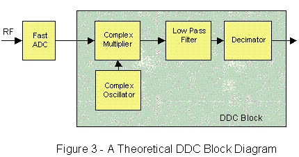
All these concepts are drawn together in the block diagram of Figure 3
How fast an ADC do I need?
The concept of the DDC is to sample the whole input signal and to use digital techniques to reduce the data. However, that may require an unrealistically fast ADC.
For example, Nyquist’s theory states that we should sample at a rate "at least double the bandwidth of interest". If we do this on a 1GHz carrier, we would need an ADC sampling at well over 2GHz; that ADC would be protected by anti-aliasing filters, removing any signal above 1GHz. However, this is beyond what can be achieved with today’s technology.
Frequency shifting is required before the ADC. This can be done in analog, using an IF stage; or it may be possible to use a composite approach.
Typically, if the signal is at 1GHz, the bandwidth of interest may be only a MHz wide. The filters required to select such a narrow band would be large and complex; but selecting a band perhaps 40MHz wide could be practical. If we can select this band using analog filters, it is possible to sample at a reduced rate – using the bandpass sampling mentioned earlier. In this case, a sample rate (Fs) of 100MHz would mean that our signal could be frequency shifted by 10Fs, bringing the 1GHz signal in at a much more reasonable 100MHz sample rate.
The more aggressively this technique is applied, the greater the strains on the anti-aliasing filters. It also places great emphasis on high analog bandwidth for the ADC, and extremely low jitter for the ADC clocks; any errors here will be magnified greatly. However, it can be used very effectively.
This technique is complementary to frequency-shifting the signal to an "Intermediate Frequency" or IF. Typically the approach used – direct conversion, IF or "bandpass sampling" will be chosen dependent on the frequencies involved and other system issues –even down to the type of antenna deployed. Most systems use a combination approach, using an analog IF stage to bring the signal down to something that can then be processed digitally.
Why would we use a DDC over Analogue Techniques?
Plainly a DDC is implementing something which could be done in analogue – it’s sometimes good to stop and check why we’d want to do this.
The DDC is typically used to convert an RF signal down to baseband. It does this by digitising at a high sample rate, and then using purely digital techniques to perform the data reduction.
Being digital gives many advantages, including:
- Digital stability – not affected by temperature or manufacturing processes. With a DDC, if the system operates at all, it works perfectly – there’s never any tuning or component tolerance to worry about.
- Controllability – all aspects of the DDC are controlled from software. The local oscillator can change frequency very rapidly indeed – in many cases a frequency change can take place on the next sample. Additionally, that frequency hop can be large – there is no settling time for the oscillator.
- Size. A single ADC can feed many DDCs, a boon for multi-carrier applications. A single DDC can be implemented in part of an FPGA device, so multiple channels can be implemented – or additional circuitry could also be added.
However, there are some disadvantages:
- ADC speeds are limited. It is not possible today to digitise high-frequency carriers directly. There are techniques to extend the range of ADCs, but often it is simpler to use analogue circuits to bring the carrier down to an IF that digital circuits can then manage.
- ADC dynamic range is limited. In many communications systems, the signal’s amplitude can vary greatly. Fast ADCs often only have 12bits of resolution – giving an absolute maximum dynamic range of 72dB. It is often better to use analogue circuits in conjunction with the ADC to implement AGC functions to ensure that this range is best used.
In time, more and more systems will use predominantly digital technology. However, the high speeds of many communication systems will ensure that a hybrid approach, using analogue and digital, will be the best route for many systems for a long time to come. The quest for more spectral space will ensure that new systems will use ever higher frequencies, ensuring that analog approaches will be around for a long time to come!
Further Reading
There are many aspects of DDCs that we have touched on lightly in this tutorial. Try the following for more information:
CIC Filters: The original paper on CIC filters is a mathematical work of art – however, that doesn’t make it useful for engineering purposes! A lighter introduction is available at:
DSPGuru - http://www.dspguru.com/info/tutor/cic.htm
This references Hogenauer’s original paper, but it’s not strictly necessary to understand all the maths to get a CIC working!Complex Maths: Another useful tutorial on the DSPguru website, complex maths explained in simple terminology – essential for a full understanding of much of communications theory:
DSPGuru - http://www.dspguru.com/info/tutor/quadsig.htmDDC Chips: Take a look at how the fixed-function DDC chips are structured. Many of these are overkill – they have to be as they need to match the needs of many users, while your design can be application specific. You can still learn from them; Graychip in particular have excellent datasheets:
Graychip has recently been acquired by Texas Instruments but you can still find their datasheets at the TI website, in the Analog & Mixed Signal section.