Home>>User Area>>Application Notes>>External Memory Types for 'C6000 Systems
External Memory Types for C6000 Systems
Introduction
The C6000 processor core can place intense demands on its memory subsystem. In any one cycle, up to eight instruction words can be fetched; in addition, two data words can be requested, while the DMA can perform a further access. With a potential maximum of eleven 32-bit accesses being performed every cycle, the chip's designers have spent considerable effort tuning the on-chip memory system for best performance.
This paper looks at what happens when code or data is placed in off-chip memory. We start by looking at the various types of memory the C6000 family supports, and the different types of memory access it can perform.
This paper does not address the cached versions of the C6000 family ('C6211, 'C6711). These will be added in a later version.
Internal Memory
Internally, a C6000 processor has dedicated RAM blocks for program and data storage. The program RAM is 256-bits wide, allowing eight instructions to be fetched in a single cycle; the data RAM is 32-bits wide, also allowing a 32-bit access every cycle. Two buses can perform read and write accesses to the data RAM, subject to certain restrictions.
On most C6000 processors, the memory is divided into multiple blocks. If the two buses access different blocks, they can both proceed in a single cycle; if they access the same block, a wait-state is inserted. Additionally, data within the blocks is interleaved; if the two accesses are to different banks of the interleave, they again complete in a single cycle.
External Memory
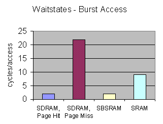
The C6000 family support three types of external RAM - Static RAM (SRAM), Synchronous Burst SRAM (SBSRAM) and Synchronous Dynamic RAM (SDRAM). The two SRAM technologies offer small, high speed memories - DRAM is typically 4-8x larger than SRAM. SRAM is a random-access memory technology using a simple "asynchronous" interface. Only two transactions are possible - Read or Write. SRAM technology offers high speed, or low power (seldom at the same time!).
The synchronous memories (SBSRAM and SDRAM) use a "clocked" interface. This interface is more complex, so a single access takes longer than with conventional SRAM; however, after the first access, subsequent accesses can be performed very quickly. These subsequent accesses do not need to be sequential, but they do need to be in the same direction - all reads, or all writes; if not, they are treated as single accesses.
 |
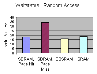 |
There are two further complications with SDRAM - pages and refresh. The SDRAM is divided into pages. For example, the HERON1-C6201 carries 16Mbytes of SDRAM, organised as pages of 256 words. The first access to the memory needs to open a page - this takes a long time. If the next access is to this open page, the memory behaves very much like the SBSRAM. However, if the access is to a different page, this must be opened first - which again takes a long time.
SDRAM also requires refresh cycles. These are special memory accesses performed to ensure that the memory contents remain valid. One must be performed in each page in the memory within one "refresh period". The first access after a refresh cycle must always open a page, so is slow. The overall effect of this is typically a 1-2% drop in system performance.
C6000 Memory Accesses
The C6000 core can perform three distinct types of memory access. These are instruction fetches, data access and DMA accesses. The cache provides additional access types, which are very similar to those of the DMA.
Instruction Fetches are always reads from memory. Instructions are grouped together in "execute packets" - a group of up to eight instructions which are executed in parallel. These are fetched as a single unit, so the processor can use a burst read access from SDRAM or SBSRAM.
Data Accesses are performed by LD / ST instructions. These stall the processor until complete; so even if there is another memory access following this one, they are always treated as single accesses by the external memory.
The DMA can perform copies of blocks of data between memory areas, or from a peripheral to memory. In these cases, memory accesses may be treated as groups, taking advantage of the fast access features of SBSRAM or SDRAM. The cache fetches instructions in exactly the same way, using a burst length of eight.
Consequences of Access Types
Burst accesses (from the DMA or CPU instruction fetch) can be performed efficiently to external memory. These can use the efficient burst modes of the SDRAM or SBSRAM. While this is significantly slower than the on-chip RAM (SDRAM is 16x slower than on-chip memory), these accesses can be efficient to load the CPU cache, or DMA data on-chip.
CPU data accesses (which NEVER use burst mode) carry a large time penalty. Wherever possible, it is more efficient to transfer the data to be operated on into on-chip RAM. If this is not possible, it may be worth considering one of the cached variants of the chip - such as the 'C6211 or 'C6711.
Practical Results
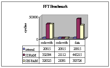
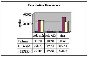
In separate papers we describe FFT and imaging algorithms. We've used benchmarks from those papers to show the effects of different memory types. To test hand-optimised code, we used the assembly-coded 16-bit integer FFT, while for C code, we used the 3x3 convolution, written in optimised C code (with intrinsics).
We timed each benchmark with the code & data internal, then with each of code and data placed externally in SBSRAM & SDRAM. The results are shown below:
Conclusions
Looking initially at program storage, we can see that placing it externally has a drastic effect on performance - giving a 16x increase in execution time on the FFT. This is to be expected - only one 32-bit instruction may be fetched from external memory at a time, and each fetch takes at least two machine cycles. In contrast, up to eight 32-bit instructions may be fetched from the internal program memory in a single cycle. The convolution sees slightly lower degradation, as it issues fewer instructions in parallel.
However both are small functions which fit easily within the cache. With the cache enabled, performance is not significantly below that of the internal memory.
For data, the processor performs all accesses as single memory transactions. The result of this is many wait-states, giving a 10-15x drop in performance for SBSRAM, and 15-20x for SDRAM; the SDRAM's lower performance being due to page misses.
For these benchmarks it would be far faster to DMA the data to on-chip memory, process, and DMA the results back to main memory. This technique can also overlap DMA transfers and processing, giving further performance enhancements.