Home>>Products>>Modules with FPGA & SDRAM>>HERON-FPGA7
HERON-FPGA7 Module

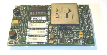
HERON-FPGA7 FPGA module with SDRAM and Digital I/O
- Xilinx VirtexÛ-II FPGA with 3, 6 or 8M gates
Need a larger FPGA? See here.- 256Mbytes of SDRAM connected as 64Mx32 @ 133Mhz
- FPGA configuration downloaded using the HERON Serial Bus.
- Choice of clocking options
- 45 user defined Digital I/Os
- 1 channel of RS232/RS485.
- Connects to all of the HERON FIFOs, UMI and module ID signals
- Flash PROM for storage of configuration data
- This module can be used with ready made IP to perform often used functions
Prices: (ex VAT & shipping)
HERON-FPGA7V3000-5: È2,582 (3M gates, speed grade 5)
HERON-FPGA7V3000-6: È3,011 (3M gates, speed grade 6)
HERON-FPGA7V6000-5: È5,317 (6M gates, speed grade 5)
HERON-FPGA7V6000-6: È6,977 (6M gates, speed grade 6)
HERON-FPGA7 is supplied without cables as standard. However, some cables can be supplied included in the hardware price, if
required. Please specify at time of ordering either up to two FPGA30 or one FPGA30-CameraLink cables. See HERON-FPGA7
cables for more information.
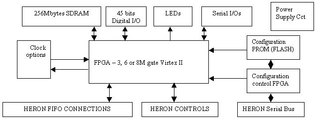
The HERON-FPGA7 provides a user programmable FPGA element for a HERON system combined with a bank of SDRAM capable of more than 500Mbytes/second. This can be used to process data flows or as a flexible digital I/O module.
Using the HERON serial bus allows the FPGA to be configured with a standard module configuration, or a custom one provided by the user or HUNT ENGINEERING. After configuration the module can accept user messages over the HERON serial bus allowing registers etc to be programmed. If a more significant programming change is required a complete new FPGA configuration can be downloaded. The FLASH based configuration PROM can load the configuration data into the FPGA when it is used in an embedded system This PROM can be programmed using the standard JTAG cable available from Xilinx (such as Xilinx Parallel cable 4 or USB-JTAG cable).
The Digital I/O has a number of voltage formats such as LVTTL or LVDS defined by the combination of a jumper setting and the configuration downloaded to the FPGA. In addition it is possible for the HERON-FPGA7 to be used as a choice of RS232, RS485 and Differential ECL serial interfaces.
The HERON-FPGA7 can access HERON-FIFOs at a rate of 32 bits per FIFO clock in AND 32 bits per FIFO clock out concurrently. For example with a FIFO clock of 100Mhz this is 400Mbytes/sec in AND 400Mbytes/sec out
The module has a 100Mhz oscillator connected to the FPGA, which can be divided or multiplied using the Digital
Clock Managers of the FPGA. Additionally there are sockets where the user can
add further Oscillator modules for specialist frequencies or jitter/stability
specifications. Of course the digital I/Os and UMIs can be used to provide
external clock sources to the FPGA. The use of a VirtexÛ-II XC2V1000fg456-4 part
allows clock rates of up to 365Mhz to be used internally in the FPGA, but the
clock rate that can be used depends on the FPGA design you generate and must be
determined using the FPGA development tools.
NOTE: Virtex II I/Os are not 5v tolerant!
HERON-FPGA7 Diagram
Technical Specification
| Processor: | VirtexÛ-II |
| Memory: | 256Mbytes as 64M x 32 at 133Mhz |
| Host Bus: | HERON |
| Maximum Dimensions: | 4.0 inches x 2.5inches x 6.5mm high. |
| Power requirements: | 5V dependent on FPGA configuration 12V Max: 0A Typ: 0A -12V Max:0A Typ:0A |
| Power Consumption/Dissipation | Max Bare FPGA package dissipation: 4.5W |
| Clocking Speed: | Max HERON-FPGA7V 365Mhz |
| I/O bandwidth: | e.g. HEPC9 400Mb/s in + 400Mb/s out |
Xilinx Foundation series tools are required to make a new FPGA configuration.
HUNT ENGINEERING provide software to download the FPGA configuration file onto the
hardware, plus configuration examples.
HUNT ENGINEERING may offer to provide your configuration file for you, but this may be
chargeable.
Need a ready made function? See the IP available for HERON-FPGA7
![]() Print
friendly version of this Datasheet
Print
friendly version of this Datasheet
(documents open in new window)
