Home>>Products>>IP for HERON-FPGA modules>>SDRAM FIFOs with HERON-FPGA7
Create SDRAM Based FIFOs with the HERON-FPGA7 Module
- Standard IP that you can download to an HERON-FPGA7V module to create two large FIFOs with the memory interface of the SDRAM providing the storage for the FIFO
- VHDL sources so that you can add your own FPGA design to this interface which uses only a small proportion of the FPGA resources
- Highly suitable for applications requiring buffering between high speed data sources
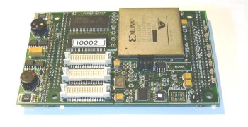
When combined with this standard bitstream, the HERON-FPGA7 splits the 256Kbytes of SDRAM memory on the module into two equal parts. Each half is used to create an individual FIFO. These two 128Mbyte FIFOs interface to two separate pairs of HERON input and output FIFOs
Typically the bitstream will be used to provide two independent FIFOs, each over 32Mlocations in depth and 32 bits wide. The first SDRAM FIFO reads and writes from HERON FIFO 0 while the second SDRAM FIFO reads and writes from HERON FIFO 1. When the HERON-FPGA7 is placed in a system with other modules and FIFOs from surrounding modules are correctly connected to FIFO 0 and FIFO 1, two large data buffers can be inserted in the flow of data through the system.
Functional Block Diagram
All I/O modules have options for cables and clocks. Please see our Cables & Clocks policy for more details.
![]() Print friendly version of HERON-FPGA7 Datasheet
Print friendly version of HERON-FPGA7 Datasheet
(documents open in new window)

